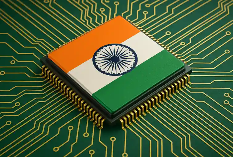
The Union Government has announced a ₹4,500 crore modernization plan for the Semiconductor Laboratory (SCL) in Mohali to upgrade its strategic capabilities, reaffirming that the facility will remain government-owned.
Modernisation of SCL Mohali
- Investment: ₹4,500 crore allocated over three years (part of the larger India Semiconductor Mission corpus).
- Strategic Status:
- No Privatisation: The facility will remain under government control.
- Role: It produces ‘Legacy Node’ chips (older technology nodes, e.g., 180nm) vital for strategic sectors like Space (ISRO), Military, and Railways.
- Key Function: Currently engaged in “Taping Out” chips designed by students under the Chips 2 Startups (C2S) programme.
- History: Once a leading facility, it lost its edge after a fire in 1989. The current upgrade seeks a “hundredfold” increase in production.
2. The Umbrella: India Semiconductor Mission (ISM)
- Nodal Ministry: Ministry of Electronics and Information Technology (MeitY).
- Launch: 2021.
- Core Objective: To build a vibrant semiconductor and display ecosystem to reduce import dependency and integrate India into the global value chain (GVC).
- The Four Key Schemes:
- Semiconductor Fabs: Fiscal support of up to 50% of project cost for setting up Silicon Fabrication units.
- Display Fabs: Fiscal support of up to 50% for TFT LCD / AMOLED display fabrication units.
- Compound Semiconductors / Sensors / ATMP: Fiscal support of up to 50% of capital expenditure for Compound Semiconductors, Silicon Photonics, Sensors, and ATMP/OSAT (Assembly, Testing, Marking, and Packaging) facilities.
- Design Linked Incentive (DLI) Scheme: Targeted at startups and MSMEs. Offers financial incentives (up to ₹15 crore) and design infrastructure support for Integrated Circuits (ICs), Chipsets, etc.
3. Supporting Initiatives
- SPECS: Scheme for Promotion of Manufacturing of Electronic Components and Semiconductors (provides Capex incentive).
- EMC 2.0: Electronics Manufacturing Clusters to provide world-class infrastructure.
- FDI Policy: 100% FDI is allowed in the electronics manufacturing sector under the automatic route.
- Chips to Startups (C2S): Aims to train 85,000 highly qualified engineers in Very Large Scale Integration (VLSI) and Embedded System Design.
Static Concepts
- Wafer: A thin slice of semiconductor substance, such as crystalline silicon, used in electronics for the fabrication of integrated circuits.
- Fab (Fabrication Plant): A factory dedicated to manufacturing integrated circuits.
- Fabless: Companies that design chips but outsource the manufacturing to a foundry (Fab).
- ATMP/OSAT: Post-fabrication services. They do not “make” the chip but package, test, and assemble the silicon wafer into a usable product.
- Taping Out: The final result of the chip design cycle/process before the design is sent to the foundry for manufacturing.